TL;DR: we reproduced Denis Andzakovic’s¬†proof-of-concept showing that it is possible to read and write data from a BitLocker-protected device (for instance, a stolen laptop) by sniffing the TPM key from the LCP bus.
Authors: Thomas Dewaele & Julien Oberson
Special thanks to Denis Andzakovic for his proof-of-concept and Joe Grand (@joegrand) for his hardware hacking teachings at Insomni’hack 2018.
Theory
Bitlocker is the Full Disk Encryption (FDE) solution offered by Microsoft for its Windows operating systems starting with Windows Vista to protect users’ data at rest. The solution offers various configurations including several ways to store the decryption key. The most common configuration consists in storing the Volume Master Key (VMK) within the Trusted Platform Module (TPM) that is embedded in recent computers.
This setup is interesting because the decryption is completely transparent to the user. This benefit surpasses others since many companies are reluctant to configure an additional password/PIN for the user to boot its computer. The downside is that it opens the door to several attacks including the TPM sniffing described in this post but also DMA or Cold Boot attacks.
Under the hood, the TPM checks various system properties during the startup to ensure that the boot sequence has not been altered. If the validation succeeds, the VMK is released and transmitted to the CPU which could start to decrypt the disk and to load the operating system.
Depending on the hardware, the TPM can be connected to the motherboard with several communication channels including LPC, I2C or SPI. These buses share a common property, namely a low transmission speed (the clock is generally around 25Mhz). This is not an issue for the solution because only a limited quantity of data has to be transmitted but it makes channel sniffing easier since required hardware is inexpensive.
Finding the TPM
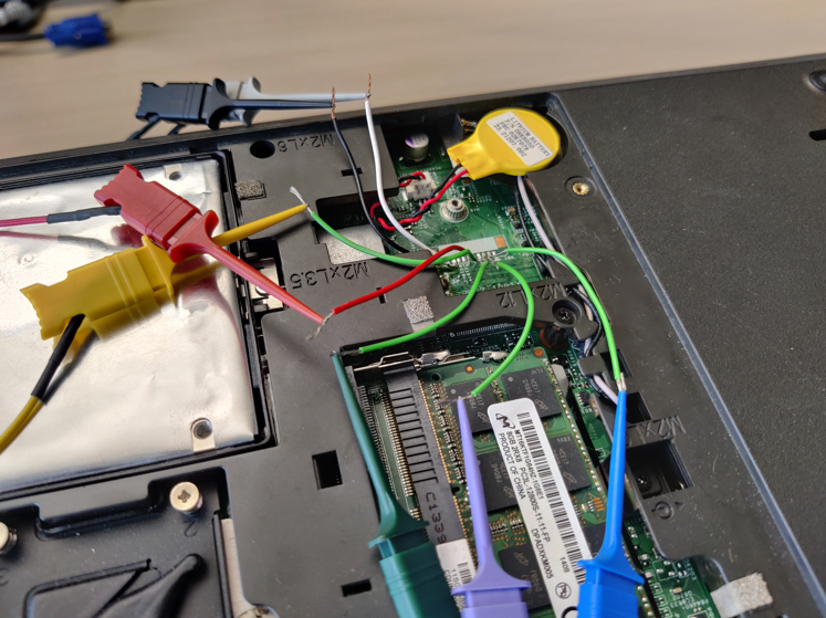
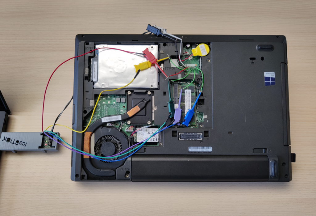
The first step to perform this attack is to locate the right place to probe. Of course, the location varies depending on each motherboard. In our case, the test subject was a Lenovo ThinkPad L440.
The best way to find the communication bus is if you can obtain the motherboard schematics, but we could only find one website that had the schematics for the L440, and it seemed a bit dodgy.
Instead, we decided to go the manual way and started our journey by locating the TPM chip. These chips usually come in TSSOP28 or VQFN32 packages. We found a TSSOP28 chip labeled P24JPVSP under the trackpad and Google seemed to indicate that it is related to TPM:
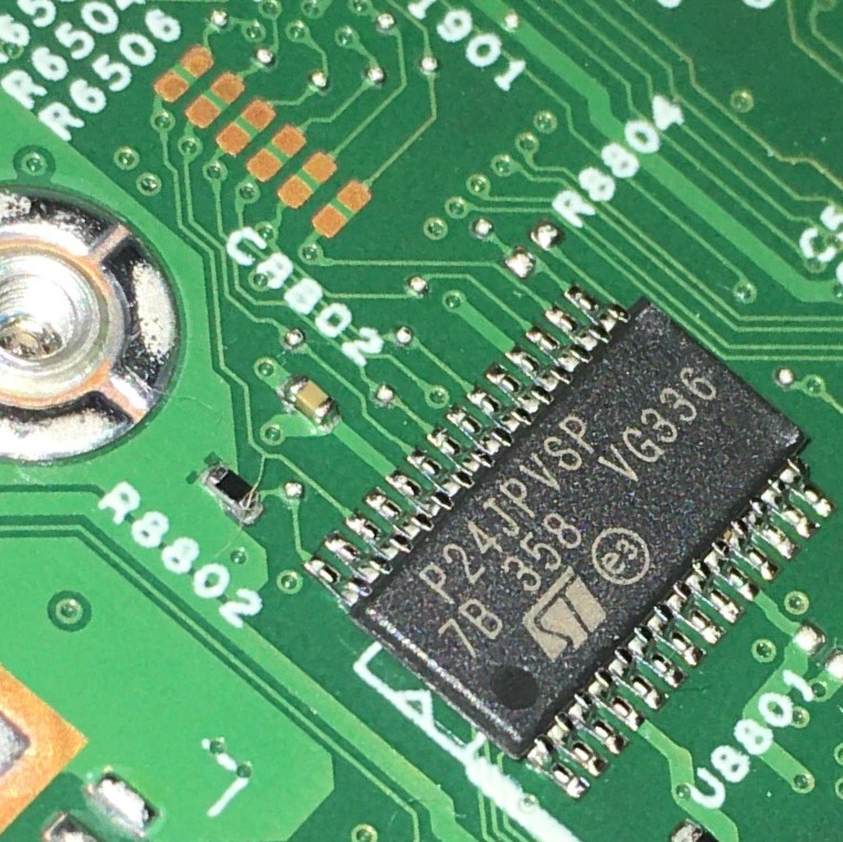
As evidenced by the logo, the chip is made by ST Microelectronics, but the reference P24JPVSP was not found on st.com. After some educated guesses and some more Google searches, we arrived to the conclusion that it is probably equivalent to the ST33TPM12LPC chip which relies on LPC for communications. Here is the pinout from the data sheet:
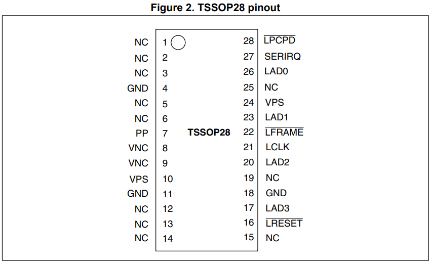
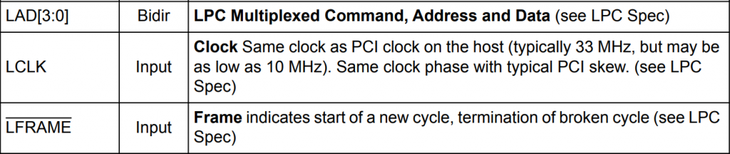
In order to retrieve the LPC frames, we need to probe the following 6 signals (+ ground):
-
LAD0,LAD1,LAD2andLAD3are the 4 bits bus where data is actually exchanged to and from the chip - The frame signal is used to indicate when individual LPC frames start or end
- The clock signal is just a cyclic tic at a constant frequency (in our case 25 MHz) that is used to synchronize all the other signals
Now, if (1) you have the correct equipment and (2) you’re confident in your micro-soldering skills, you can solder wires directly on these pins to attach the probes, but the space between each pin is only 0.65 millimeters (for our metrically impaired readers, this is 0.4 millionths of a mile). We did not meet several of these two requirements.
Fortunately, it is not uncommon to find more convenient places on the board that are connected to these pins. As you can see in the picture above, there are 6 pads directly next to the chip, and you can follow the traces to get the following pinout:
1 2 3 4 5 6
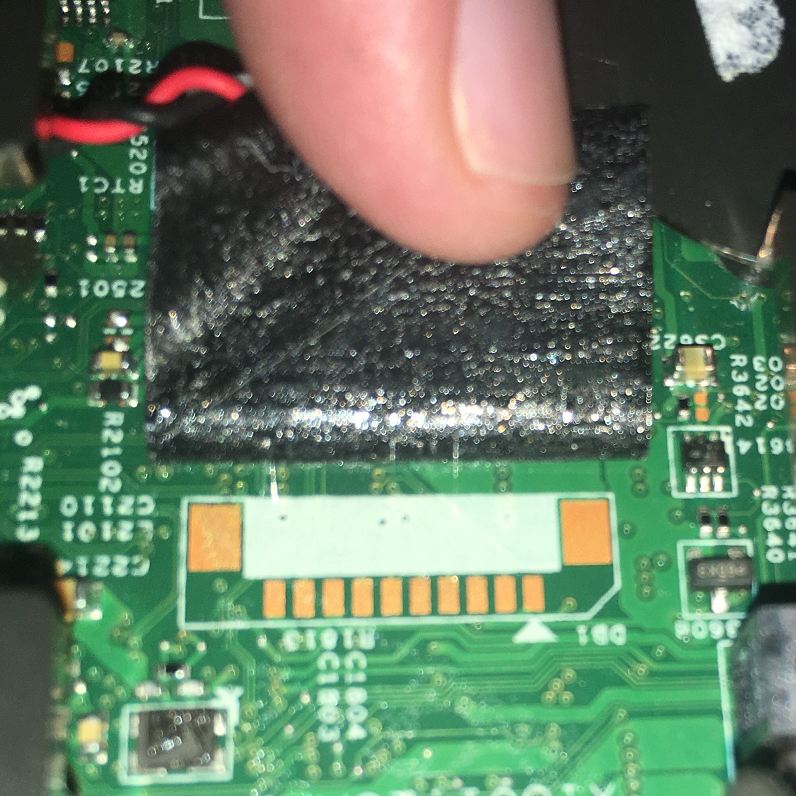
LAD0 LAD1 LFRAME LAD2 LAD3 LRESETUnfortunately, the LCLK signal is missing! It seems that the trace going to this pin is coming from the other side of the motherboard. On the bottom side, this is located under the WiFi module, and it was initially covered by black tape:
We were happy to discover these (relatively) big LPC debug pads, meaning that not only we should have an easier time soldering probes there, but also we can perform the attack by just removing the bottom panel without the need to disassemble the whole laptop and keyboard assembly.
Using a multimeter in continuity mode, we determined the pinout of these pads (which was a bit acrobatic since the chip is on the other side of the board). Unfortunately, we were still missing LCLK, and one of the pads did not seem to be connected to anything. We thought that this was too big a coincidence and surely this unknown pad was actually LCLK, except the circuit is going through some resistors between the pad and the pin.
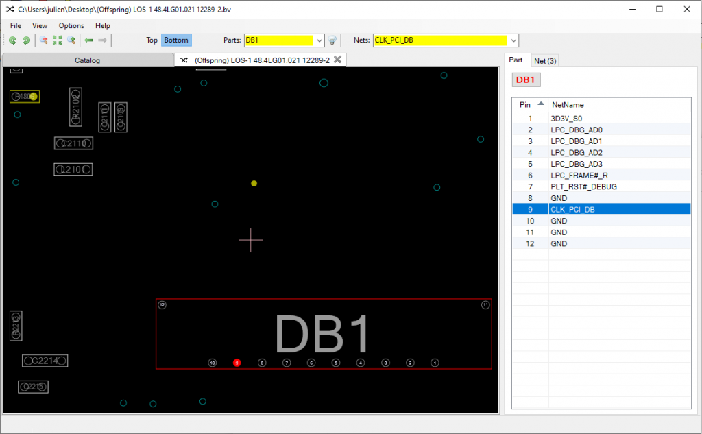
At this point, we could have probably YOLO’ed it and hoped that our assumption was correct, but we thought that we would actually try to purchase the motherboard schematics from the strange website mentioned at the beginning.
We paid the $20 over PayPal, fully expecting to get scammed, but 15 minutes later, we received an email from a GMail address with some .rar archives containing the BoardView file and software. Naturally, we opened the archives and ran the software on our production domain controller, and it was actually legit! We could confirm that the mystery debug pad was indeed the LPC clock going through some resistors and through a BGA mounted chip (we would have had a tough time doing continuity tests under there!)
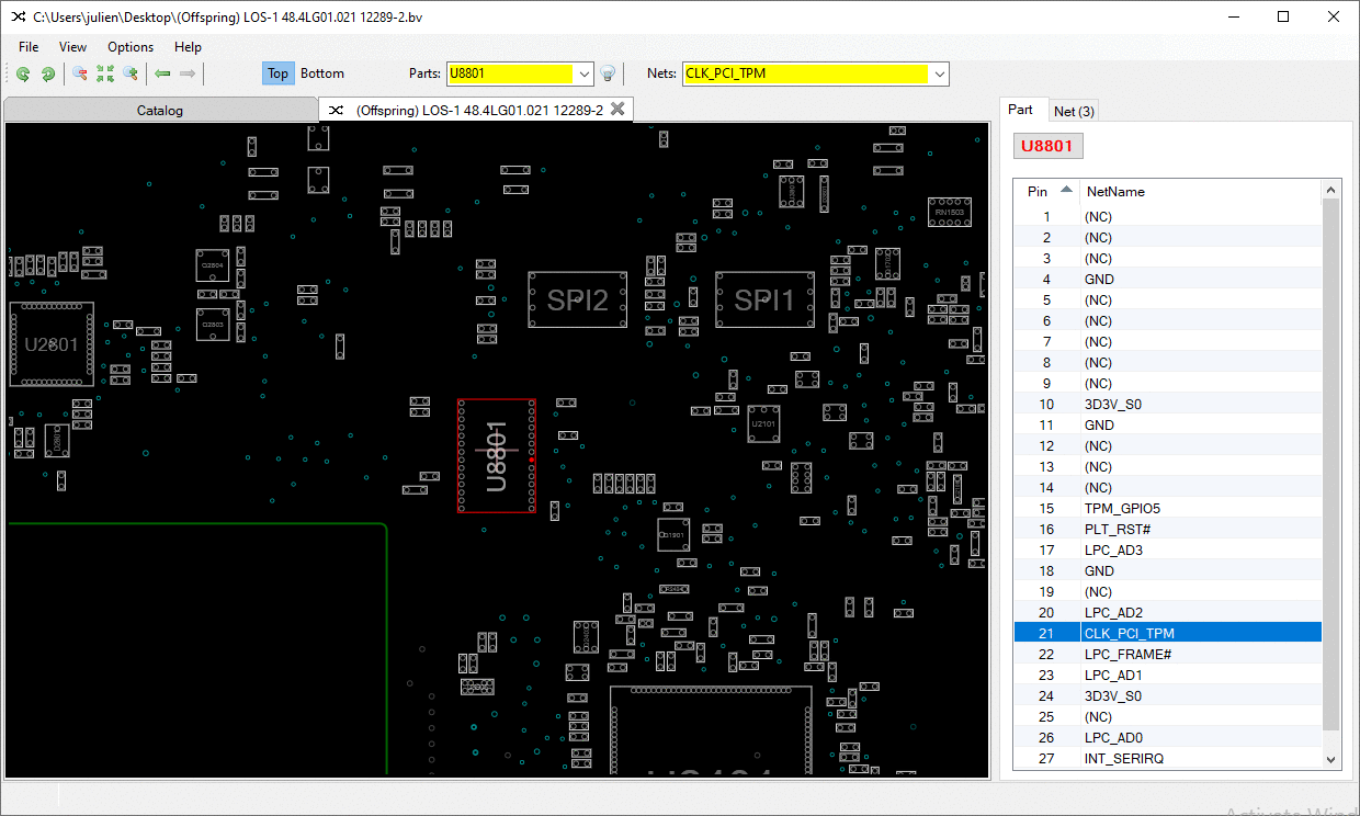
Below is the pinout of the LPC debug pads, and we finally have all the required signals. We also noticed, thanks to the schematics, that the clock signal path from the chip to the debug pad was not complete and we had to create a soldering bridge to link them (cf. resistor R1806).
Hooking up a sniffer
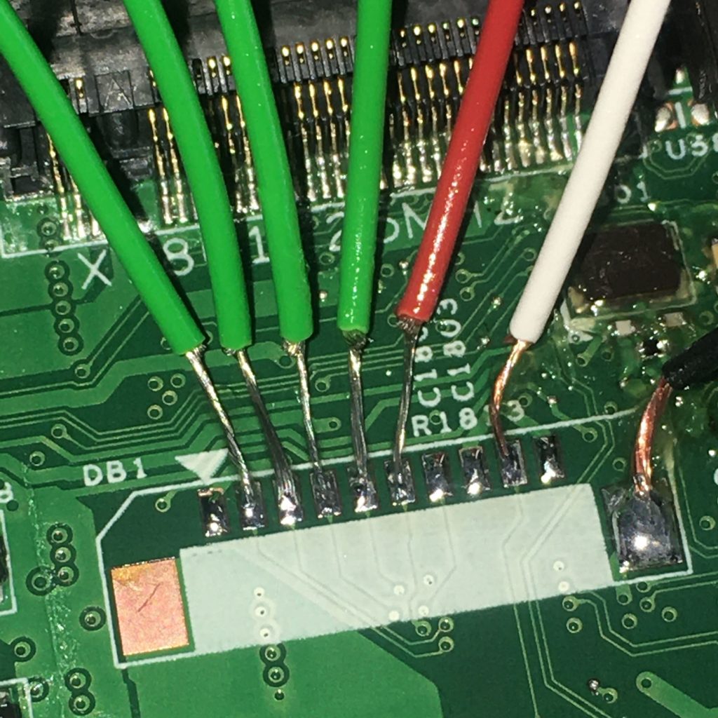
After finding the best location to probe, we soldered some wires to the LPC debug pads in order to easily hook the sniffer.
We started by connecting a MSO 19.2 logical analyzer in order to observe the traffic. According to the manufacturer’s data sheet, the LA buffer is not large enough to capture the whole starting sequence so the device was only used to verify that data were properly retrieved. By doing so, we were able to confirm that the signal shape matched LPC traffic.
In order to circumvent the buffer limitation, we used an FPGA-based device produced by Lattice Semiconductor namely the iCEstick40. This is the same hardware that Denis Andzakovic used for the TPM 2.0 sniffing attempt (except ours is enclosed in a fancy-home-3D-printed box!)
We connected the sniffer according to the pinout specified in the LPC sniffer Github repository using probe clamps to the previously soldered wires. The clamps ensured a good connection with the soldered wires but the connection to the sniffer module was less reliable. In order to reduce movements and therefore limit contact issues, the plugs were tightened by compressing the lower part of the metal connector.
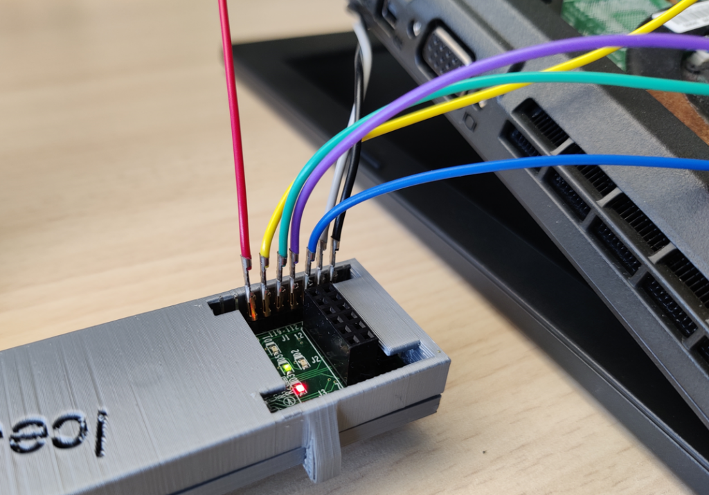
VCC 3.3|NC 1
GND        2
lpc_clock  3
lpc_ad[0]  4
lpc_ad[1]  5
lpc_ad[2]  6
lpc_ad[3]  7
lpc_frame  8
lpc_reset  9
Data acquisition
The data acquisition was performed using a modified version of the LPC Sniffer. The firmware was modified by Denis Andzakovic to save buffer storage and therefore delay overflow by only recording TPM-related addresses 0x00000024.
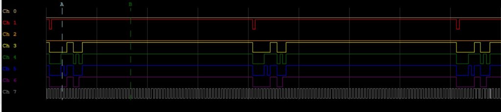
After flashing the device, the read_serial.py python script can be used to retrieve the LPC frames. The following command is executed on the sniffing computer, then the target laptop was turned on in order to let the TPM check PCR registers, release the VMK and transmit it over the LPC bus.
As depicted in the output below, only the frames that starts with 24 are recorded in the output log file.
$ sudo python3 parse/read_serial.py /dev/ttyUSB1 | tee log1
[snip]
b'000000240000'
b'000000240000'
b'000000242c00'
b'000000240000'
b'000000240000'
b'000000240000'
b'000000240100'
b'000000240000'
b'000000240000'
b'000000240000'
b'000000240300'
b'000000242000'
b'000000240000'
b'000000240000'
b'000000245a00'
b'00000024f900'
b'000000244900'
b'000000240900'
b'000000241600'
b'000000240100'
b'000000243a00'
b'000000240b00'
[snip]
Once the boot sequence is completed the script is stopped. The collected data were processed to remove the frame header and only keep the actual data. Then the grep command is used to extract the VMK header followed by the key (32 following hexadecimal characters) as shown below.
$ cut -f 2 -d\' log6 | grep '24..00$' | perl -pe 's/.{8}(..)..\n/$1/' | grep -Po "2c0000000100000003200000(..){32}"
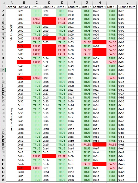
2c00000001000000032000005af9490916013a0bc177b3301d41508c4af8abb8583de5e4c60bbbabafad8a3aThe key values observed on the bus were not exactly the same every time. This behavior is probably related to the sniffer connection which is far from perfect even after the socket tightening session. As the transmission errors occur randomly, it was relatively easy to identify them by comparing multiple measurements. The table below illustrates the values obtained during four boots.
Disk decryption
With the decryption key in hand, it was possible to decrypt the local disk thanks to dislocker. The last version of the tool at the time of writing is 0.7.2 and it supports the --vmk option which allows to directly specify the VMK without having to reconstruct the FVEK. The VMK has to be placed in a binary file as shown below.
$ hexdump -C vmk
00000000  5a f9 49 09 16 01 3a 0b  c1 27 b3 30 1d 41 50 8c
00000010  4a f8 ab b8 58 3d e5 e4  c6 0b bb ab cf ad 8a 3a
$ sudo dislocker -v -V /dev/sdb3 --vmk vmk -- /media/bl
$ sudo mount -o ro,loop /media/bl/dislocker-file /media/blm
$ ls /media/blm
'$RECYCLE.BIN'             ESD            pagefile.sys    'Program Files (x86)'         Users
'$SysReset'                hiberfil.sys   PerfLogs         Recovery                     Windows
 Chocolatey                install        ProgramData      swapfile.sys
'Documents and Settings'   Intel         'Program Files'  'System Volume Information'
At this point it would be possible to circumvent completely the Bitlocker protection and typically :
- access and tamper any stored file;
- steal the local password database including;
- local accounts in the SAM hive
- the last ten domain connected users thanks to MSCACHE
- backdoor the machine with a malware
Conclusion
To summarize, we were able to retrieve the Bitlocker key in a couple of days with a 49$ FPGA module by only using tools available in DIY stores and, cherry on the cake, without breaking the computer. The operation was easier than expected especially considering it was our first hardware attack and that many companies rely on a TPM-only configuration.
Of course none of this would have been possible (at least not in such a short time) without the work of many other security researchers that discovered the issue, wrote papers and published their tools.
The motherboard schematics was a great help in finding the mapping of the debug pads. It is, however, important to highlight that better soldering skills would have allowed attaching connections directly on the TPM chip itself thus making unnecessary to trace the connections.
Recommendation
In order to avoid being targeted by the TPM sniffing attack, the easiest way would be to configure Bitlocker to use an additional pre-boot authentication factor like a PIN. Some other factors like USB devices or smartcards would also work but are generally considered less convenient for the user. Of course this configuration change implies that users would have to enter an additional piece of information when to computer boots.
The recently released Windows 11 OS requires the use of a TPM 2.0 chip which was designed to offer encrypted communications. This prerequisite might open the door to a proper way of securing the transmission without requiring the user from adding a second authentication factor. Note, however, that this change would technically prevent TPM sniffing but not other physical attacks.
Additional details regarding Bitlocker countermeasures can also be found on a dedicated Microsoft post.